Beam Reduction Factors

Factors That Reduce the Beam Below the Specimen

The user of an electron microscope has a number of ways to control the intensity of the electron beam before it interacts with the specimen, most of which are illustrated elsewhere on the Electron Microscopy Center (EMC). Different things can also happen to the electron beam that reduce the beam's intensity after it passes through the specimen. For example, post-specimen apertures and an energy filter result in the loss of electrons that travel beyond that position along the optical axis of the microscope. These effects will cause the imaging systems below the specimen to report fewer electrons than actually interacted with the specimen. It is therefore important to remember that when estimating the dose that the specimen receives, it is critical to minimize anything below the specimen that (inadvertently) reduces the number of electrons reported.

However, it can be critical (in terms of producing the best possible image) to use various features of the electron microscope that reduce the intensity of the electron beam after it interacts with the specimen. This page is just a reminder of what happens to the electron beam in terms of its intensity when various things are done. The EMC offers an explanation of how energy filters operate and their effect on images, and a brief description of how post-specimen apertures affect images and the details of the different sets of apertures on the EMC's JEOL JEM 3200FS. Effects limited to the intensity of the electron beam caused by the post-specimen apertures and the energy filter (whose locations in the 3200FS are shown in the diagram to the right) are illustrated below using the 3200FS and the Gatan UltraScan 4000 CCD camera.

Different Ways to Change the Electron Beam Intensity Above the Specimen

Post-Specimen Apertures

All post-specimen apertures increase contrast in Transmission Electron Microscopy (TEM) images. They do this by causing some scattered electrons that leave the specimen to not recombine in the final image, violating the conditions necessary to produce a phase contrast image: since a perfect phase contrast image has no contrast, deviations from perfection can create contrast. Since this loss of electrons in the final image is a result of scattering by the sample, it should be clear that post-specimen apertures only effect the intensity of the electron beam when a specimen is actually in the path of the electron beam, and that the more electrons a specimen scatters, the stronger the effect of any given aperture. The effects of objective apertures on beam intensity are illustrated below using both a continuous carbon film (low atomic number, Z) and a Au/Pd replica diffraction grating or "waffle grid" (high Z).

The Electron Microscopy Center's JEOL JEM 3200FS has two sets of post-specimen apertures. The different apertures are at slightly different locations along the optical axis of the 3200FS and are referred to as the High Contrast Apertures (HCA) and the Objective Lens Apertures (OLA, also referred to as the "in gap apertures"). The details of the two aperture systems differ and there can be reasons when one is better than the other (e.g., the OLA is better than the HCA at quenching some effects of electron beam induced charging because it is physically closer to the specimen than the HCA). However, both of them cause changes in the intensity of the electron beam after it passes through the specimen, as illustrated in the High Contrast Aperture Effects plot graph.

High Contrast Aperture Effects plot graph

High Contrast Apertures (HCA)

The High Contrast Aperture Effects plot graph shows the effect on beam intensity of inserting the different high contrast apertures. The data are expressed as the percentage of mean counts in an image with no aperture in place as a function of the aperture position (where the zero position indicates no HCA aperture and the numbers 1 through 4 indicate smaller and smaller apertures). The red +'s show this effect when the specimen is a standard Au/Pd waffle grid is and the green x's show the effect when it is a simple carbon film. The carbon film, which scatters less due to the low atomic number of carbon, exhibits less of an aperture-induced reduction in beam intensity.

NOTE: The resolution at which the HCA apertures eliminate data from the powder diffraction pattern obtained from the same sort of standard waffle grid used for the data in the plot above. That figure shows that strong powder diffraction rings are eliminated by all four high contrast apertures. Based on the strong overall loss of scattered electrons shown in that figure, it is not surprising to see an almost 20% reduction in beam intensity when imaging the waffle grid using HCA #1 (the largest aperture, which still eliminates some strong diffraction rings) and a nearly 40% reduction in beam intensity when imaging the waffle grid with HCA #4 (the smallest aperture).

Objective Lens Aperture Effects plot graph

The Objective Lens Aperture Effects plot graph shows the effect on beam intensity of inserting the different objective lens apertures. The data are expressed as the percentage of mean counts in an image with no aperture in place as a function of the aperture position (where the zero position indicates no OLA aperture and numbers 1 through 3 indicate smaller and smaller apertures). The red +'s show this effect when the specimen is a standard Au/Pd waffle grid and the green x's show the effect when it is a simple carbon film. The carbon film, which scatters less due to the low atomic number of carbon, exhibits less of a reduction in beam intensity than is seen with the waffle grid.

NOTE: The resolution where the OLA apertures eliminate data from the powder diffraction pattern obtained from the same sort of standard waffle grid used for the data in the Objective Lens Aperture Effects plot graph. That figure shows that the largest aperture (#1) does not eliminate any strong powder diffraction rings while the two other (smaller) apertures do. Furthermore, the scattered electrons eliminated by both the 3rd HCA and 3rd OLA are very similar, with the OLA #3 aperture allowing slightly more electrons to pass further along the microsocope column. This is reflected in the fact that the percent of beam intensity from these two aperures is very similar: ~70% for the HCA and ~73% for the OLA.

Energy filters

Energy filters can be used either to generate a spectrum of the electrons that have interacted with the specimen and have lost energy (electron energy loss spectroscopy, or EELS), or to form an image from electrons that have an "energy chacteristic" that the user has selected. For example, the location and width of the energy slit can be adjusted to select only the electrons that have lost little or no energy (the so called zero loss peak, or ZLP, electrons) or the electrons that have lost energy due to interaction with a specific element such as carbon.

The overall shape of an energy loss spectrum is that of a Gaussian ZLP region followed by a broad and irregular region of plasmon energy loss. A relatively small exponential falloff extends from the ZLP region far into the energy loss spectrum (and the plasmon region rides on top of this falloff). This exponential falloff is additionally punctuated by "edges" created by inner electron shell ionization events associated with the elements in a given sample. For a typical thin specimen, the vast majority of electrons will be found mainly in the ZLP and plasmon regions of the energy loss spectrum.

Energy Filter: Slit Width Effects on Mean Counts plot graph

In terms of the discussion here about changes in beam intensity below the specimen, it should be clear that when images are formed using a sub-set of the electrons that pass through the specimen, the intensity of the electron beam that exits the energy filtered must be reduced relative to the intensity of the beam that enters it. The magnitude of this effect will depend on both characteristics of the actual specimen (e.g., thickness and atomic composition) and on the energy window (wavelengths) selected to form the image.For example, the fraction of electrons that interact with a given element will be miniscule relative to the overall electron beam while for a typical thin specimen, on the order of 90% of the incident electrons simply do not interact with the specimen at all (and are thus part of the ZLP electrons).

The Energy Filter: Slit Width Effects plot graph shows the percentage of the average counts in an image (relative to the image recorded without an energy slit) as the width of the energy slit is changed. The red +'s correspond to data from images of a standard Au/Pd waffle grid while the green x's correspond to data from a continuous carbon film. The experimental conditions were such that the energy slit was centered at its narrowest position (10 eV) and then simply opened wider and wider in 10 eV steps (the plot below compares the energy slit width relative to an actual energy loss spectrum recorded on a different sample). This extends the low energy side of the slit into the region of "negative energy loss" (a totally meaningless term) but makes the data collection much easier. In addition, when using a relatively narrow energy slit (for example, cryoTEM imaging often records ZLP images with the energty slit set to 20-40 eV), centering the slit at the narrowest possible width and then opening it wider eliminates issues with slight drift in the position of either the slit or the spectrum.

Superposition of Slit Width onto Typical Electron Energy Loss Spectra plot graph

As the Energy Filter: Slit Width Effects plot graph shows, an energy slit with a width between 150 and 200 eV imposes a small but fairly consistent reduction in average counts in an image (compared to the same image recorded without an energy slit). The plot to the left, Superposition of Slit Width onto Typical Electron Energy Loss Spectra, shows horizontal bars representing energy slits from 10 to 100 (black bars, bottom to top) and 110 to 200 (red bars, top to bottom) superposed onto typical EELS spectra where nothing (blue trace) or a lacy carbon film (green trace) is in the beam path. For the experimental setup used here, slit widths of 150 to 200 eV (the region where decreasing the slit width had minimal effect on the average counts) is at the high energy end of the plasmon region (usually defined as less than 50 or 100 eV, and clearly seen as the second (right-most) green peak in the plot at the left). For the images used to create the plot above, this 75 to 100 eV region is likely to include mainly electrons in the slow exponential falloff referred to above. As the slit grows narrower, it eliminates more of the plasmon electrons from the final image. The narrowest slit used here should eliminate not only all the plasmon electrons, but likely also eliminates some electrons in the ZLP region (depending on the exact energy spread of the elastically scattered electrons and whether the slit is centered symmetrically around the zero point). Also, it is clear from the plot above that the waffle grid creates more electrons that have lost energy (inelastic) than the continuous carbon film does. This is due to the scattering properties of low atomic number elements such as carbon when compared to higher atomic number elements such as Au and Pd.

NOTE: For the JEOL JEM 3200FS, slit widths of 10 to 20 eV shrink the diameter of the electron beam that passes through the energy filter and forms the filtered image enough that the CCD is not fully illuminated by the beam. This means that the average counts in such images were determined from sub-regions of the full image, and the exact sub-region used will have an effect on the measured average counts (especially for the 10 eV slit, where a large part of the CCD frame is not illuminated by the beam at all.

Beam Intensity Loss in Elastic Electrons

Mean Counts of Elastic Electrons vs Total histogram

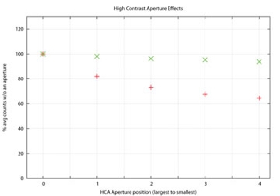
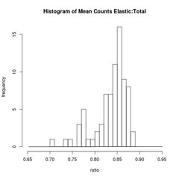
Another way to think about the loss of beam intensity due to filtering out inelasticaly scattered electrons is to examine the ratio of the mean counts in an image when only elastic electrons are collected vs the mean counts in the same image when all electrons are collected. The histogram to the right shows this ratio calculated from over 75 image pairs recorded from a standard Au/Pd waffle grid using the 3200FS during calendar year 2014. Elastic images were acquired using a 30 eV energy slit (centered with the slit set to 10 eV) and the 2nd image was acquired immediately afterwards simply by removing the energy slit. Given that the images were recorded from several different waffle grids (and at different locations on each of the individual waffle grids) and were recorded over an entire year during which the electron beam varied in intensity due to issues with the field emission gun (FEG), this distribution is relatively tight, with a mean ratio of 0.835 (± 0.038) and a median value of 0.847. This value is similar to the measurement in the plot above showing the loss in beam intensity when the energy slit width was set at 30 eV, and indicates that under these conditions, ~15% of the incident electrons consistently lose some amount of energy as they pass through a typical Au/Pd waffle grid.

NOTE: For pure elements and some well characterized compounds (and possibly some mixtures of materials), it is possible to use such image pairs to estimate the thickness of the specimen. This is based on the fact that the differences between an image formed from all the electrons (no energy slit) and an image formed from only elastically scattered electrons (a narrow energy slit, e.g., 10 to 20 eV) are due to the removal of the inelastically scattered electrons, and thus the image pair quantifies the amount of inelastic scattering. If one knows or can estimate the inelastic scattering properties of the specimen, it is possible to correlate this measured amount of inelastic scattering with the thickness of the specimen. This correlation is referred to as a thickness determination, and an image generated in this manner is referred to as a thickness map.

The key to generating an accurate estimate of thickness is knowing the average distance an electron can travel in any given material before inelastic scattering occurs (a quantity referred to as the inelastic mean free path). In fact, if the inelastic mean free path is known, the following formula can be used to determine the thickness of the material in question:

thickness = MFPinelastic * ln( I0 / IZLP )

where thickness = specimen thickness (in the units of the MFP)
MFP = mean free path (usually measured in nm)I0 = total incident electron
IZLP = electrons in the zero loss peak
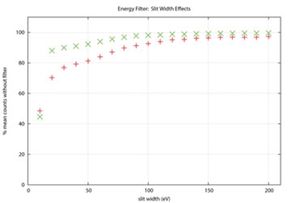
NOTE: the ratio I0 / IZLP is the inverse of what is shown in the histrogram above

For the Au/Pd waffle grid used to produce these data, the inelastic mean free path will depend on the exact thickness of the carbon support film and both the exact thickness and the exact atomic composition of the Au/Pd layer. In general, these are unknown quantities and thus exact thickness measurements are not possible in this case. In such cases, the formula shown above is often rearranged to produce a fractional ratio of the (unknown) inelastic mean free path:

ratio = thickness / MFPinelastic = ln( I0 / IZLP )
where ratio is in fractional units of MFPinelastic

However, the fact that the ratios shown above are reasonably consistent means that these properties are relatively consistent both in different locations of an individual waffle grid and between different waffle grids.

Beam Intensity Loss Due to cryoEM

Yet another commonly encountered loss of beam intensity due to the energy filter occurs when working with a frozen, hydrated sample (cryoEM), and it can be important to know typical energy loss effects for such samples. The inelastic mean free path in ice of an electron accelerated to 300 kV is about 350 nm (Grimm et al., 1996). Although many if not most grids prepared for cryoTEM will have ice layers that are thinner than this, ice thicknesses on the order of 100 nm or thicker are typical for many frozen Quantifoil and C-flat grids (i.e., just under one third of the inelastic mean free path of a 300 kV electron). When attempting cryo tomography, it is also possible to observe grids where the thickness of the sample and the ice exceeds the inelastic mean free path several fold, and it is critically important to realize when this happens.

Ice Thickness vs Zero Loss Peak (ZLP) Electron Beam Intensity plot graph

The graph to the right shows the intensity of the zero loss peak (ZLP) electron beam (measured as a percentage of the incident electron beam) as a function of the thickness of the layer of ice that the beam encounters. For a thickness on the order of 100 nm of ice (fairly typical for cryoEM grids), the intensity of the electrons in the ZLP is ~75% of the incident electron beam. When the thickness grows to 350 nm (one inelastic mean free path, marked with a black arrow on the graph), the intensity of the beam is further reduced to less than 40% of the incident electrons. As the ice grows thicker, the intensity of the ZPL electrons drops further, and when thicknesses greater than two inelastic mean free paths are encountered, the ZLP intensity drops to less than 15% of the incident electron beam.

Another way to think about this graph is that if one knows the approximate ratio of the ZLP beam to the incident beam (the beam without any of the post-specimen apertures mentioned above or the energy slit), it is possible to get a crude estimate of the thickness of the ice. Various people using the EMC have collected cryoEM image pairs that can be used in this fashion, though in most cases the images contain a mixture of ice, protein and the carbon support film (where the protein and carbon film can significantly alter the assumed inelastic mean free path). With that warning in mind, and using statistics based on the entire images instead of selecting areas that only contain ice and protein, users of the EMC report ratios that range from 0.30 to 0.75 (~420 nm to ~100 nm, assuming the inelastic mean free path of pure ice is applicable), with a mean of ~0.49 ± 0.11 (~250 nm, ranging from 180 to 340 nm). It would be useful to collect this sort of information for every cryoEM data set, and to determine whether there is a correlation between "thin ice" determined this way and the quality of reconstructions generated from such images.

Changes in Magnification

It should also be noted that when the microscope's magnification is changed without adjusting the diameter of the electron beam, (fairly) consistent changes in beam intensity should result. In a perfect electron microscope, the spread of the electron beam across the specimen would not change as the magnification is changed and the magnifications reported by the instrument would be exact. However, the number of electrons that interact per unit area of any image recording device (phosphor screen, film or some sort of CCD) will depend on the magnification of that image. In other words, when magnification is raised without adjusting the electron beam, the phosphor screen (or any sort of image recording device) will interact with fewer and fewer electrons on a per unit area, causing the resulting image to grow dimmer.

This is simply a function of optics and magnification. For example, doubling the magnification causes the area illuminated by the beam to increase four-fold (and thus spreads the same number of electrons per unit time over an area that is four-fold larger). Large changes in magnification can cause images to be much too dim (i.e., the magnification was raised too high without re-adjusting the size of the electron beam, and too few electrons are interacting with the image recording device) or much too bright (i.e., the magnification was lowered too much without re-adjusting the size of the electron beam, and too many electrons are in the resulting image). Lowering the magnification significantly can even cause the beam to be so bright at the CCD that potential damage to the device can occur.

Changes in Magnification plot graph

This effect is illustrated in the Changes in Magnification plot, where average counts in an image (as a percentage of the counts in a blank CCD image recorded at 25,000x) are plotted as the magnification is doubled (from 25,000x to 50,000x) and doubled again (from 50,000x to 100,000x). The first doubling should reduce the counts to 25% of the original value and the second to 25% of the value at 50,000x (6.25% of the original value). For our 3200FS, the change from 25,000x to 50,000x results in a slightly stronger reduction (to ~22%) than what is expected (25.0% of the original) while the change from 25,000x to 100,000x results in a slightly weaker reduction (to ~7.5%) than what is expected (6.25% of the original). This deviation from an ideal system is not likely to be caused by actual changes in the size of the electron beam as it interacts with the specimen, but rather is most likely caused by slight deviations between the actual and reported magnifications on the 3200FS. However, please keep in mind that if the magnification changes involve lenses other than the projector lenses (below the specimen), it is possible for the actual size of the electron beam to change also as the magnification is changed.

Remember that the effect described immediately above is actually an apparent change in beam intensity: the intensity of the electron beam that interacts with the specimen is not altered when the magnification is changed, nor are any fewer electrons passing along the optical axis to the detector(s). It can be very important to account for this effect when imaging a sample at a defined electron dose (e.g., imaging frozen, hydrated biological samples that damage in the electron beam): although the electron dose is defined by the user, situations may arise where the optimal magnification to use is high enough that the number of electrons interacting with the film/camera/etc. becomes limiting in terms of the signal-to-noise in the resulting image quality.