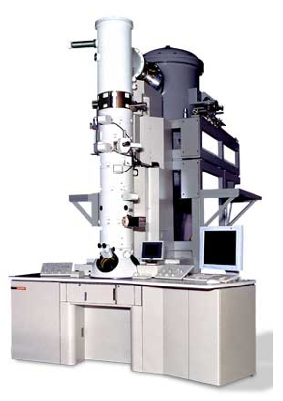
JEOL JEM 3200FS

Field Emission Gun (FEG)

The electron source of the 3200FS is a thermal (Schottky-type) field emission gun which  generates electrons through a phenomenon called quantum tunneling. The type of quantum tunneling used in FEG's uses a strong electrostatic field at a very sharp tip (usually zirconium oxide coated tungsten, as shown in the image at the right) to release electrons. Schottky-type FEG's are thermionic emitters similar in some ways to the tungsten and LaB6 filaments used in many TEM's. However, FEG's generate several orders of magnitude more electrons than these other electron sources, and can therefore create a much brighter and more coherent electron beam.

Our FEG uses a filament current to heat the emitter, an extraction voltage to create the quantum tunneling effect and a second applied voltage to suppress the electrons thermally released from the device. Once electrons have been released from the tip, they are accelerated into the rest of the electron microscope by yet another (variable) applied voltage. The 3200FS can operate at voltages below 300 kV, but it actually performs best when this final voltage is maintained at 300 kV and the lower accelerating voltages are created by inserting electrical shorts that decrease the final acceleration by 100 or 200 kV. Other voltage adjustments can then be made to the accelerating voltage around these set points (100, 200 and 300 kV), allowing the user access to any desired accelerating voltage. The 3200FS is currently aligned for work at both 300 kV and 100 kV. If other accelerating voltages would be beneficial, please contact the staff.

Transmission Electron Microscopy (TEM) Imaging

Most users of the 3200FS will perform some sort of transmission electron microscopy (TEM) imaging. What this really means is that the instrument is operated so that a beam of electrons goes from the FEG into a series of electron lenses and forms a plane wave of electrons that then passes through the specimen. This electron wave is collected, focused and magnified by additional electron lenses below the specimen. The ray diagram to the right shows the lenses below the specimen that are involved in TEM image formation. The images formed are phase contrast images, and there is a huge amount of electron optical theory behind how this all works.

TEM of this sort is occasionally referred to as conventional transmission electron microscopy (cTEM or CTEM), especially in the context of other slight modifications of this normal imaging process. There are many "flavors" of CTEM that differ in both subtle and not so subtle ways from one another, and the rest of this section deals with different types of CTEM that can be performed using our 3200FS.

In the field of materials science, the term high resolution TEM (HRTEM) is often used. The essence of HRTEM is that the TEM and image recording devices are operated so that structural features such as the atomic lattice of "hard materials" (electron beam insensitive materials) can easily be seen in the images themselves. This generally involves high magnifications (100,000x to 500,000x), especially when recording the images using a slow scan CCD such as our Gatan UltraScan 4000. Most transmission electron microscopes built in the last 5-10 years are capable of HRTEM imaging for samples with features such as the layering of graphite (3.4 Å), while TEM's with accelerating voltages of 200 and 300 kV can usually image the smaller atomic lattices of metallic nanoparticles (e.g., Au's atomic spacing is 2.35 Å).

Another slight modification of CTEM imaging is cryo transmission electron microscopy (cryoTEM or simply cryoEM). When performing cryoTEM, the electron microscope is operated in the normal imaging mode, but the specimen itself is maintained near the temperatrure of liquid nitrogen (-196 °C or 77 °K) using specially designed specimen holders that are generally cooled using liquid nitrogen. This low temperature minimizes (but cannot eliminate) radiation damage effects on soft materials (especially unstained biological samples) and must also be used in conjunction with other methods to minimize damage from the electron beam. Some recent TEM's (such as the JEOL JEM 3200FSC and the FEI Tecnai G2 Polara) can even hold specimens at temperatures near that of liquid helium (-269 °C or 4 °K). Just to make life confusing, recent use of the term cryoTEM really extends to imaging any sort of specimen (cooled or even room temperature) using techniques to minimize radiation damage or even to CTEM imaging of room temperature biological specimens where extensive image processing is done after the images are acquired...

Finally, the 3200FS is capable of energy filtered TEM (EFTEM). When performing EFTEM, the in-column energy filter is used to separate the electron beam into it's different energies (wavelengths), to select only a particular energy range for further analysis (i.e., to filter the electron beam based on its energy or wavelength) and to recombine only those selected electrons into an image. The resulting image can be formed from only the electrons that have not scattered at all (a so-called zero loss peak, ZLP, image), or it can be formed from only those electrons that have inelastically scattered from a particular element. An image can also be formed from the electrons that have lost only 50-100 eV (a plasmon image). The use of the energy filter for EFTEM makes this technique less comparable to CTEM than HRTEM or cryoTEM, but it still fundamentally uses the electron microscope as a conventional image forming device: electron lenses form a plane wave of electrons that interacts with the sample, and other electron lenses collect, focus and magnify the scattered electron wave.

Gatan UltraScan 4000 CCD Camera

The 3200FS has a 4k x 4k Gatan UltraScan 4000 CCD camera mounted below the camera chamber. This camera has a dynamic range of 16-bits and utilizes 15 micrometer pixels with a 4 port readout. The multi-port readout makes it possible to record a full 4k x 4k image within 10-12 s (i.e., approaching the ease and speed of recording onto film), meaning that more time is spent examining the specimen and adjusting imaging conditions while less time is spent actually recording the images.

We have not explicitly determined either the modulation transfer function (MTF) or detector quantum efficiency (DQE) of this camera, but our magnification series demonstrates that there is considerable signal near the Nyquist frequency in 4k x 4k images recorded using the UltraScan camera.

In-column Energy Filter (aka "Omega Filter")

Energy filters for EFTEM and EELS can be placed in two fundamentally different locations along the electron optics of any given electron microscope:

Post-column Energy Filters

In this arrangement, the energy filter is below the specimen viewing chamber (if present) and below the cameras normally associated with a conventional TEM (i.e., the plate camera and most slow scan CCD devices). The Gatan Imaging Filter (GIF) is the most commonly encountered such device. The normal arrangement of a post-column filter is to bend the electron beam through 90° well below the normal film plane and to place the energy filter and its detectors along a vector running parallel to the floor and exiting the back of the electron microscope.

When a post-column filter is used, there is an appreciable "post-film plane" magnification factor (on the order of 10-15x) due to the added path length through the energy filter and its detectors. Because of this additional path length, it can be difficult to record images that are identical except for the use of the filter (i.e., images that differ only by the wavelengths of the imaging electrons).

In-column Energy Filters

In this arrangement, the energy filter is below the specimen but above the viewing chamber and above the usual cameras. Such filters are often referred to as "omega filters" due to the path that the electron beam must follow as it passes through the filter.

The electron beam always passes through the in-column energy filter and "energy filtering" occurs only when a slit is inserted into the beam path. Because there is no additional path length when the slit is inserted, in-column energy filters make it extremely easy to record images  that are identical except for the use of the filter. On the other hand, because the electron beam always passes through the energy filter, any image degradation caused by the lenses in the energy filter will occur all the time.

Our 3200FS uses an in-column filter that can be controlled either by TEMcon (JEOL's software that talks directly to the 3200FS) or by DigitalMicrograph (Gatan's software that talks to the microscope and to the various detectors attached to it). In addition to the software control for the detailed behaviour of the energy filter, there are several knobs and buttons on the left-hand knobset that control some fundamental aspects of the filter (i.e., whether the slit is inserted or not, the applied energy offset, etc.).

This ~30 cm long in-column filter is located right above the specimen chamber and is the main reason that the airlock for introducing specimens into the column of the 3200FS is more than 2 meters from the floor!

Electron Energy Loss Spectroscopy (EELS)

When an electron beam hits a thin specimen, the majority of electrons in the beam (90% or more) do not interact at all. The rest scatter either elastically or inelastically (no energy loss or some energy loss, respectively). The energy filter described above can be used to form images composed of electrons that have no energy loss (i.e., those electrons that were scattered elastically) or electrons that have a specific energy loss (electrons that have scattered inelastically from a specific element such as carbon). The energy filter can also be used as a spectrophotometer that measures the distribution of electrons as a function of energy. Many processes can cause inelastic scattering, but for EELS, the best understood of them involves the ionization of inner shell electrons by the electron beam.

The imaging mode mentioned above is called "energy filtered transmission electron microscope" (EFTEM) and is described in more detail here (along with some example images). The spectroscopy mode is referred to as "electron energy loss spectroscopy" (EELS) and is decribed here. The essence of EELS is that when inner shell electrons are ionized by the electron beam, there is a characteristic loss of energy that is specific for both a particular element and a particular atom's electronic state. This characteristic energy loss means that an element will have peaks at energy loss values corresponding to the different electronic orbitals, and the energy loss fine structure of the peaks themselves reveals information about the electronic state (e.g., chemical bonding state). Analysis of the spectrum therefore both shows the elements in the specimen and gives information about the electronic configuration of those elements. Changes in the EELS spectrum in different areas of the specimen reveal changes in both composition and electronic configuration (though thickness effects must also be carefully considered).

Scanning Transmission Electron Microscope (STEM) Imaging

The 3200FS is not only equipped for high resolution TEM imaging of biological and materials science specimens, but it also has the scan coils and detectors necessary for bright field (BF-) and high angle annular dark field (HAADF-) scanning transmission electron microscopy (STEM). Such dual purpose instruments are often described as (S)TEM's or S/TEM's, where "(S)" or "S/" indicate that this is not a dedicated STEM instrument, but rather capable of both TEM and STEM.

When operating in STEM mode, the electron beam is focused into a small point on the specimen. As the beam is rastered across the specimen, the forward scattered electrons at each raster point are counted and the resulting electron counts and x/y locations on the specimen are turned into an image. If the detector that collects the electrons is situated so that the counted electrons have only been scattered by a small amount, the image is referred to as bright field STEM (BF-STEM). A BF-STEM detector is essentially a disk that sits along the optical path of the instrument. The electrons that form BF-STEM images include those that cause effects such as diffraction contrast and bend contours in a conventional TEM image, and BF-STEM images are formed from "coherent electrons" (i.e., electrons that are interacting with each other).

When the detector that counts the electrons is placed so that it only counts electrons scattered through larger angles, the image is referred to as dark field STEM (DF-STEM). Since such a detector must exclude the electrons scattered at lower angles, it must be an annulus. There are generally two types of DF-STEM detectors, which differ only in the scattering angles that are sampled. A dark field detector that collects electrons scattered at slightly higher angles than those found in BF-STEM images is generally simply called a dark field STEM detector (and the images it forms are referred to as DF-STEM). DF-STEM images can also include electrons involved in things like diffraction contrast. A detector that only collects very highly scattered electrons is generally called a high angle annular dark field STEM detector (and the images it forms are referred to as HAADF-STEM images). The figure to the left shows the relative locations of STEM BF, DF and HAADF detectors.

The 3200FS has both a bright field and a high angle annular dark field detector. The number of electrons that have been scattered to the high angles collected by the HAADF detector is a function of both the atomic number of the atoms and also the number of atoms along the electron beam's path. This dependence on atomic number (Z) has lead to the use of "Z-contrast images" as an alternate name to "HAADF-STEM images." Changes in specimen thickness will also be reflected in the Z-contrast images, and HAADF-STEM analysis always needs to include thickness measurements if the interpretation of the Z-contrast can be affected by any changes in specimen thickness.

Energy Dispersive X-Ray Spectroscopy (aka EDX, EDS or EDXS)

As mentioned above, when the electron beam interacts with a specimen, electrons can either scatter elastically (i.e., with no change in energy) or inelastically (i.e., with some amount of energy loss). There are different types and causes of inelastic scattering (each with its own individual scattering cross-section), and (for example) our energy filter can detect electrons that have lost energy due to inelastic scattering.

Another result of inelastic scattering is the production of X-rays.

STEM combined with EELS or EDX

Whenever an electron beam hits the specimen, multiple things happen. These include both elastic and inelastic scattering events. In turn, the inelastic scattering events can be caused by various physical processes and can result in both the obvious energy loss of the incident electrons and phenomena such as Auger and secondary electrons and the X-rays described above.